

Most of us will probably have seen semiconductor wafers as they trundle their way through a chip factory, and some of us may have wondered about why they are round. This roundness is an obvious problem when one considers that the chip dies themselves are rectangular, meaning that a significant amount of the dies etched into the wafers end up being incomplete and thus as waste, especially with (expensive) large dies. This is not a notion which has escaped the attention of chip manufacturers like TSMC, with this particular manufacturer apparently currently studying a way to make square substrates a reality.
According to the information provided to Nikkei Asia by people with direct knowledge, currently 510 mm x 515 mm substrates are being trialed which would replace the current standard 12″ (300 mm) round wafers. For massive dies such as NVidia’s H200 (814 mm2), this means that approximately three times as many would fit per wafer. As for when this technology will go into production is unknown, but there exists significant incentive in the current market to make it work.
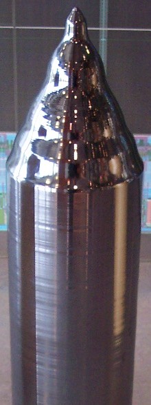
As for why wafers are round, this is because of how these silicon wafers are produced, using the Czochralski method, named after Polish scientist [Jan Czochralski] who invented the method in 1915. This method results in rod-shaped crystals which are then sliced up into the round wafers we all know and love. Going square is thus not inherently impossible, but it will require updating every step of the process and the manu ..
Support the originator by clicking the read the rest link below.


